25+ digital signal processing block diagram
P025 is a GPIO digital. Download Free PDF Download PDF Download Free PDF View PDF.
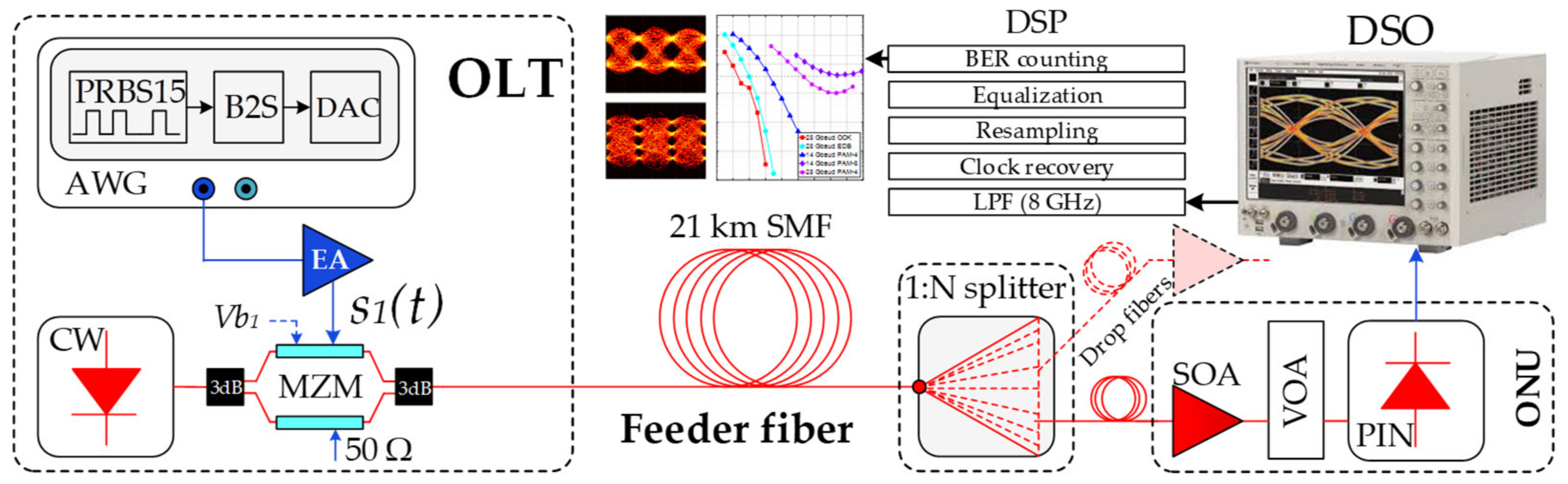
Applied Sciences Free Full Text Optical Power Budget Of 25 Gbps Im Dd Pon With Digital Signal Post Equalization Html
Proj 28 Floating point Arithmetic Logic Unit.

. Proj 27 VLSI Systolic Array Multiplier for signal processing Applications. Proj 26 ON CHIP PERMUTATION NETWORK FOR MULTIPROCESSOR. The design of radar transmitterreceiver affects these three parameters directly.
The below diagram indicating the Amplitude shift keying block diagram. 8086 is a 16-bit microprocessor and was designed in 1978 by IntelUnlike 8085 an 8086 microprocessor has 20-bit address busThus is able to access 2 20 ie 1 MB address in the memory. TRACEPKT2 is a trace packet bit-2 standard inputoutput port by the inner pull-up.
Digital Signal Processing An Introduction with MATLAB and Applications Copy. Proj 32 SMART SENSOR. Download Free PDF Download PDF Download Free PDF View PDF.
Proj 25 CRC Circuit Architecture. The clock input provides the basic timing for processing operation and bus control activity. As we know that a microprocessor performs arithmetic and logic operations.
Proj 30 FFT Processor Using Radix 4 Algorithm. A central processing unit CPU also called a central processor main processor or just processor is the electronic circuitry that executes instructions comprising a computer programThe CPU performs basic arithmetic logic controlling and inputoutput IO operations specified by the instructions in the program. Ω 4π σ.
Analog signal processing unit wireless data transmission unit and digital processing unit. This pin requires the microprocessor to terminate its present activity immediately. Their research focused on the transmission system design.
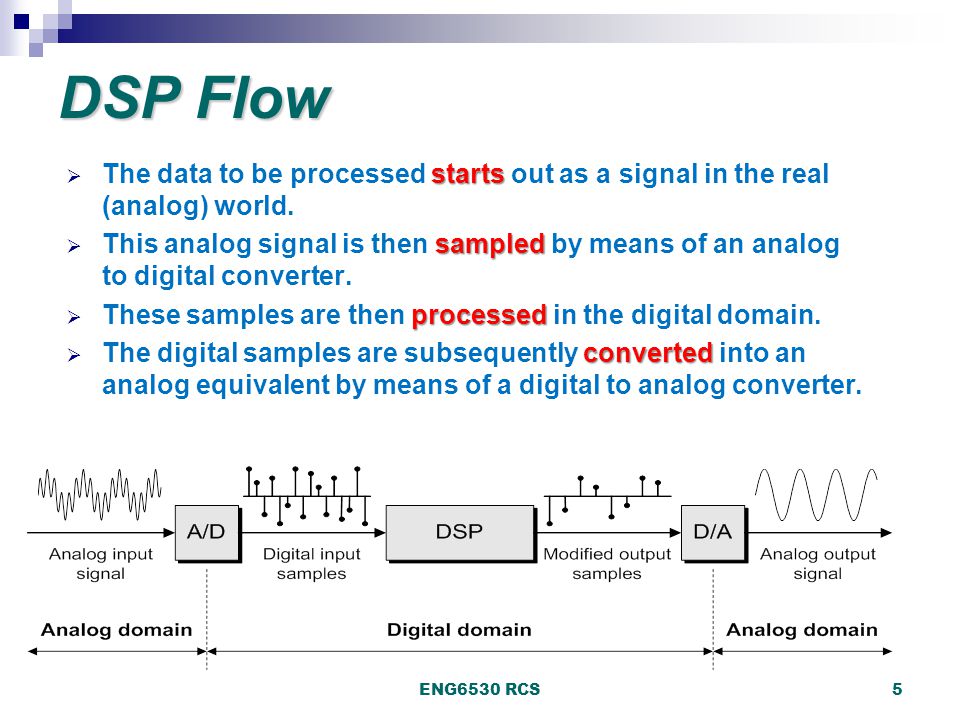
Signals to be processed come in various physical formats that include audio video or any analog signal that carries information such as the output signal of a microphone. Av Lower system losses L Minimize system temperature T. Digital Signal Procg in Power System Protection and Ctl - W.
This contrasts with external components such as main memory. At Mixer Circuit Level When the switch is closed for all the logic HIGH time intervals ie. To represent this signal digitally the signal is sampled at fixed and equal intervals.
Digital Signal Processing DSP is the mathematical manipulation and processing of signals. Solutions Manual for Digital Signal Processing using Matlab -Second Edition. Proj 31 bit RISC Processor.
Bandwidth is the difference between the upper and lower frequencies in a continuous band of frequenciesIt is typically measured in hertz and depending on context may specifically refer to passband bandwidth or baseband bandwidthPassband bandwidth is the difference between the upper and lower cutoff frequencies of for example a band-pass filter a communication. Digital Signal Processing Library Double Arrows a la Chef EPC flow charts Fault tree Finite impulse response filter Flowchart Inertial navigation system. It is divided into three parts.
Both Cortex-M4-based STM32F4 Series and Cortex -M7-based STM32F7 Series provide. Radar range equation for search SN signal to noise ratio SN of target can be enhanced by Higher transmitted power P. P118 is a GPIO digital pin.
Proj 29 DDR SDRAM CONTROLLER. Its an asymmetric square wave with a 33 duty cycle. The set of values 1 2 4 7 18 34 25 23 35 37 29 42 41 25 and 22 measured at the sampling points.
Power Supply 5V DC GND. When the input signal having logic 1 during those intervals the switch is closed and it is multiplied with the carrier signal which is generating from the function generator for. Gravitational Wave Signal Processing.
The signal must be active high1 for at least four clock cycles. This pin is an analog voltage power supply 33V and this voltage is very useful for the on-chip analog to digital converters and digital to analog converters. Rebizant et al Springer 2011 BBS.
S 4 av e s. By the design concept of the system on a chip the chip has achieved goals of low cost low power consumption and minimizing layout area. Block diagram of Third order noise shaper in Compact Disc Players.
Full PDF Package Download Full PDF Package. R k T L P A t SN. Consider the continuous signal as shown in the figure 11.
Av average power. And an 8086 microprocessor is able to perform these operations with 16-bit data in one cycle. The continuous signal is sampled at 15 fixed and equal intervals.
What Is A Computer Block Diagram Quora
Digital Signal Processing Using Fpgas Ppt Download

All You Need To Know About A Signal Generator And How To Select One Function Generator Block Diagram Digital Signal Processing
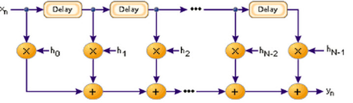
What Is Fir Filter Fir Filters For Digital Signal Processing
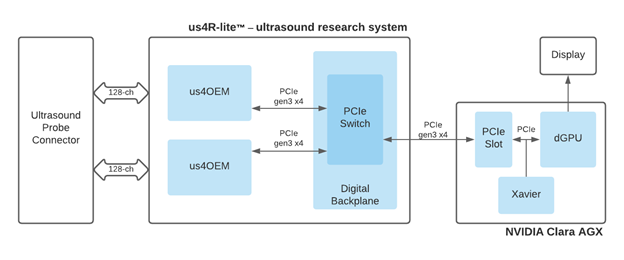
Developing End To End Real Time Applications With The Nvidia Clara Agx Developer Kit Nvidia Technical Blog
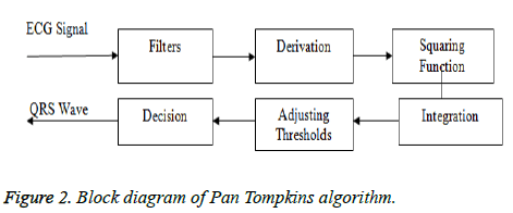
Ecg Signal Classification And Parameter Estimation Using Multiwavelet Transform
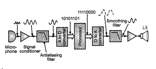
Digital Signal Processor Architecture Types Working Its Applications

An Introduction To Digital Signal Processing Digital Signal Processing Signal Processing Digital
2

Analog Dialogue Digital Signal Processing 101 An Introductory Course In Dsp System Design Part Digital Signal Processing Signal Processing Analog Devices
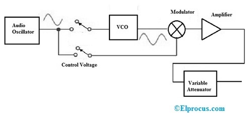
Signal Generator Circuit Working Types And Its Applications

Rockwell Collins Dsp Receiver Example Block Diagram Receiver Digital

Audio Signal Processing Using Time Frequency Approaches Coding Classification Fingerprinting And Watermarking Signal Processing Coding Quadratics
Digital To Analog Converter Dac Architecture And Its Applications
Understanding The Fundamentals Of Digital Communications National Instruments Coding Signal Processing Block Diagram
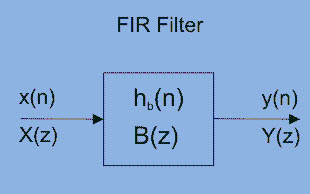
What Is Fir Filter Fir Filters For Digital Signal Processing
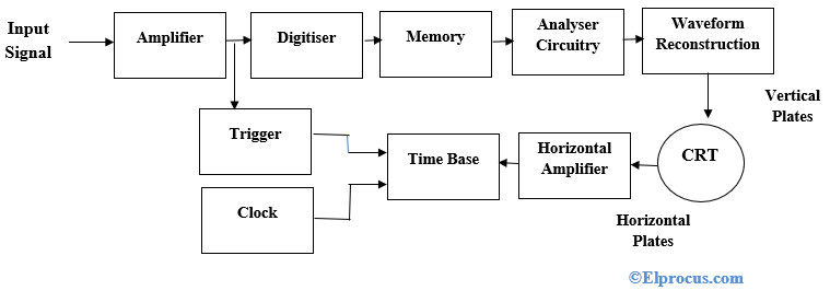
Digital Storage Oscilloscope Block Diagram Working And Its Applications